ONLINE ACCESS
Access overview
Application procedure
Online access forms
For industry
F.A.Q.
FACILITIES
Instrumentation
Methods
Map
RESEARCH
Case studies
News/Highlights
Publication list
Modules
User projects
Gallery
OUTREACH
Visits
Education
“Learning corner”
ABOUT
What is ARTEMI
Contact us
Organization
Funded by
Documents
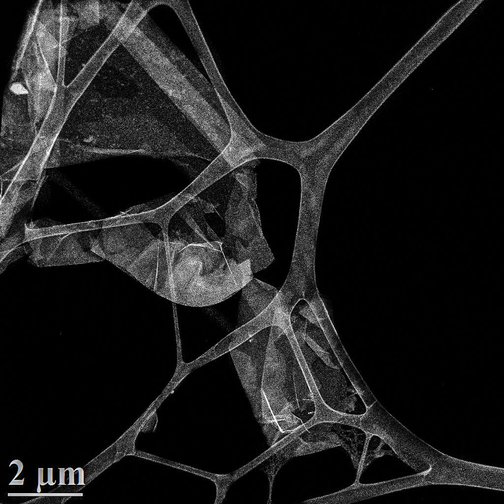
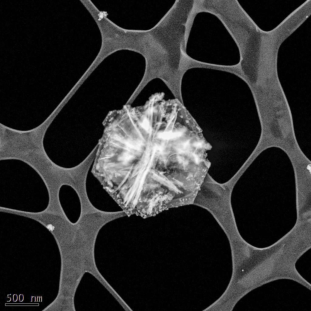
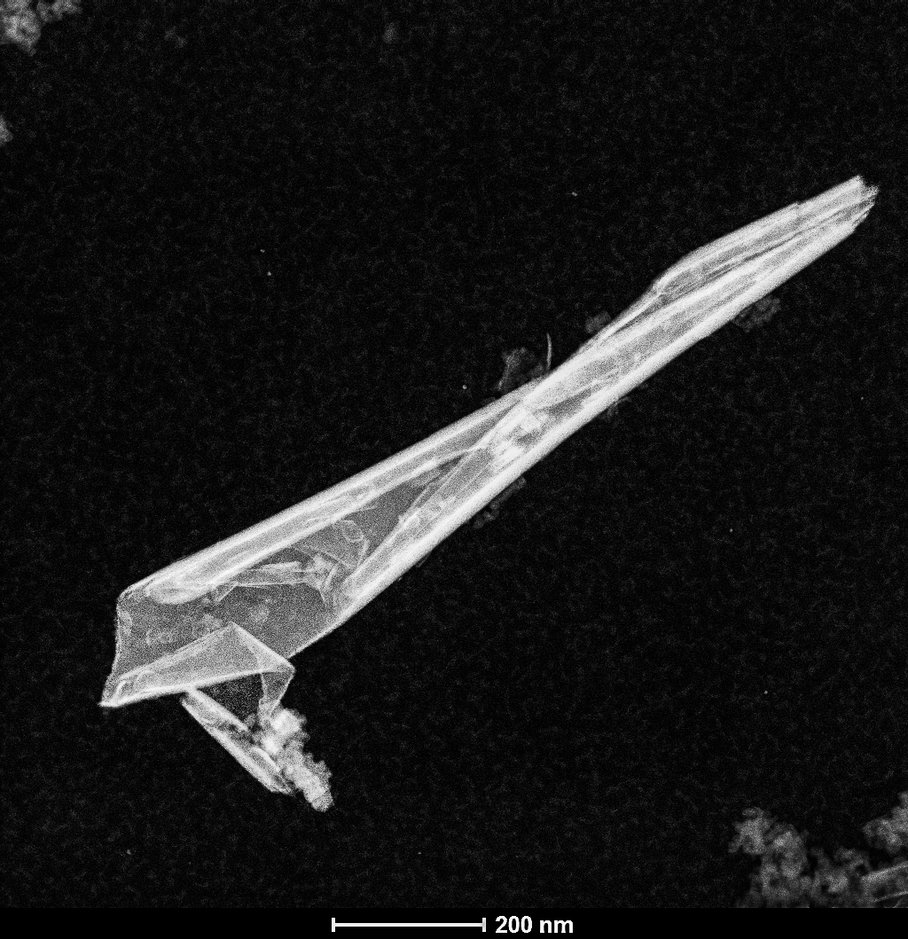
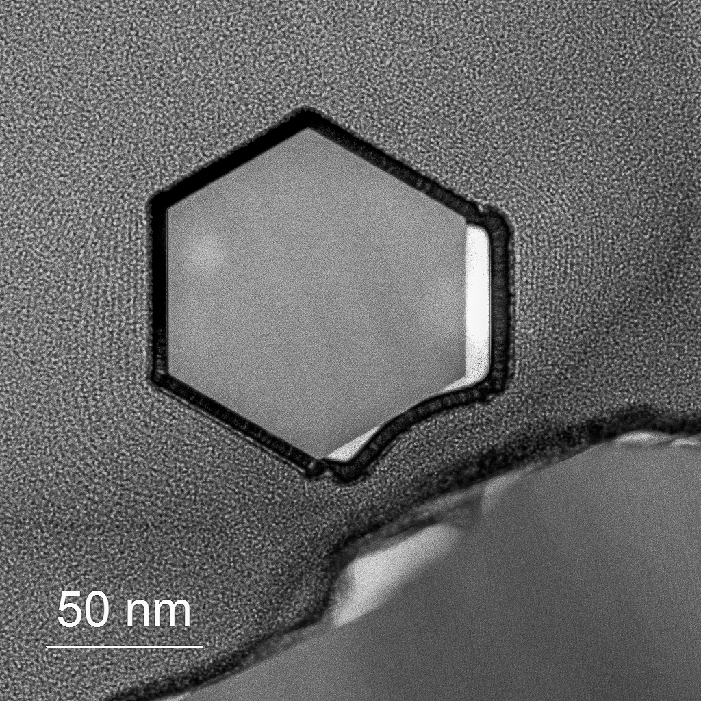
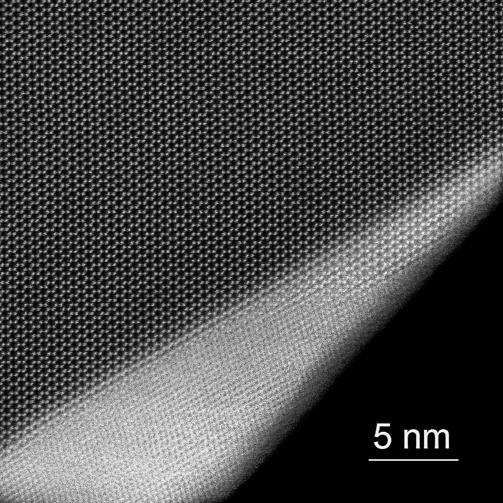
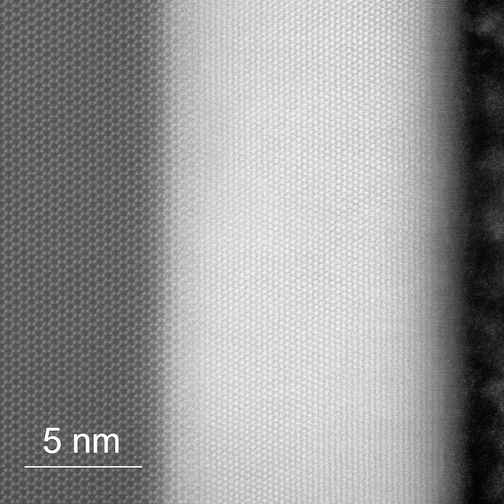
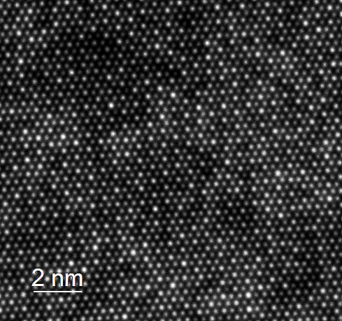
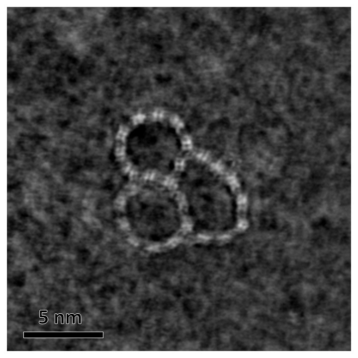
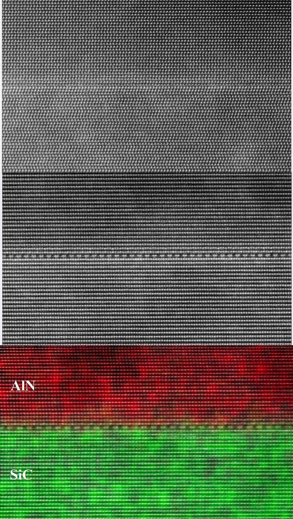
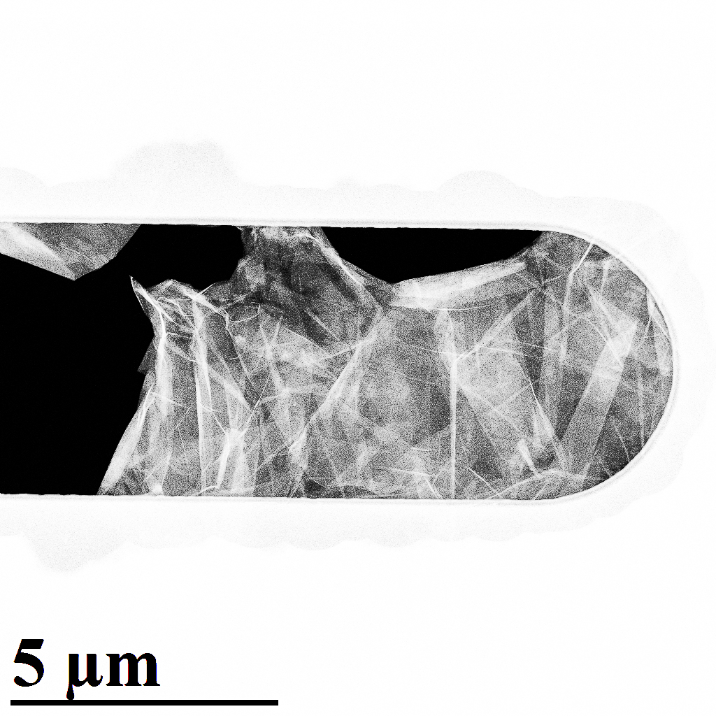
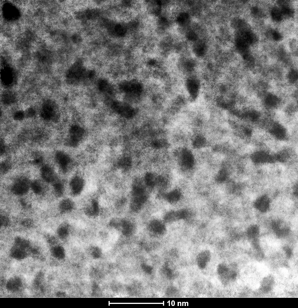
Gallery
7


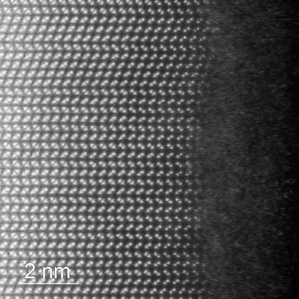
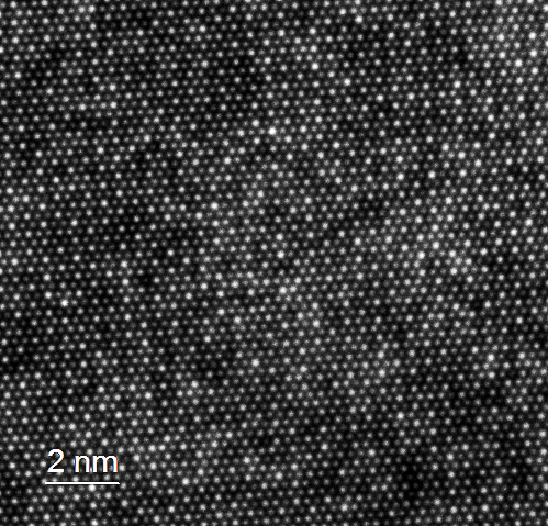
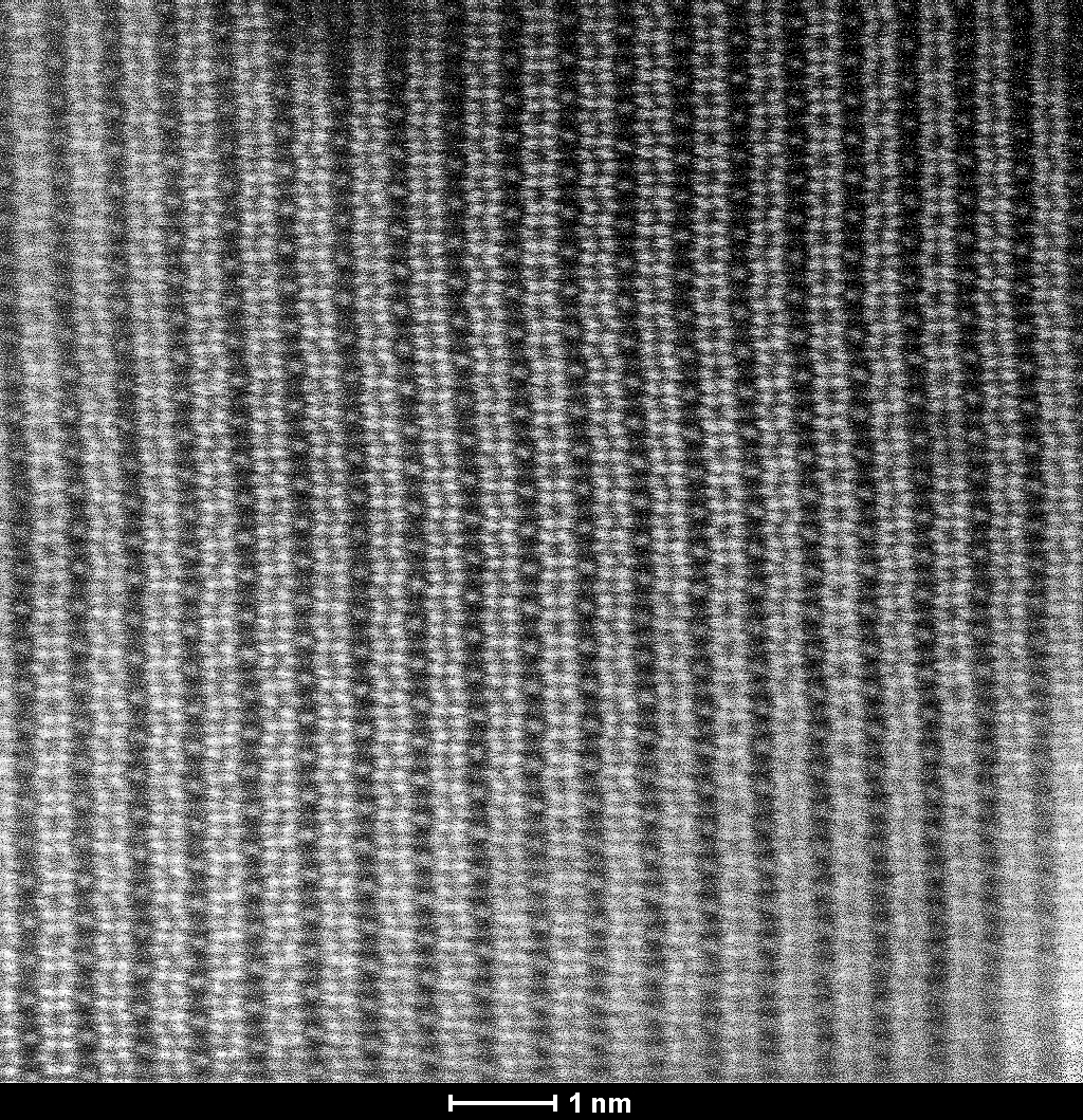
![Cr1.3sc0.7AlC [100], [010]](https://artemi.se/wp-content/uploads/2024/04/Cr1.3sc0.7AlC-100-010.jpg)
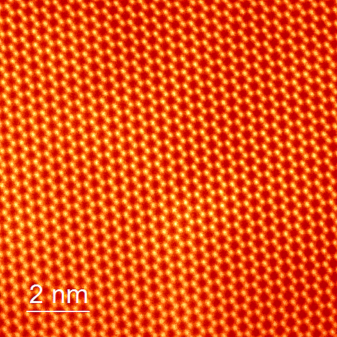
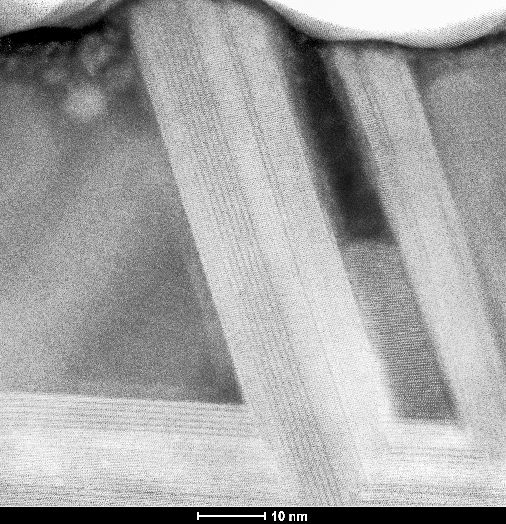
![Cr2V2AlC3 [11-20]](https://artemi.se/wp-content/uploads/2024/04/Cr2V2AlC3-11-20.jpg)


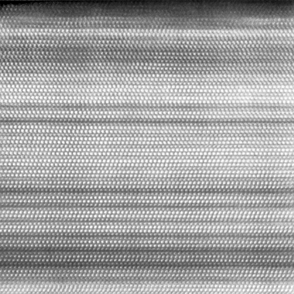

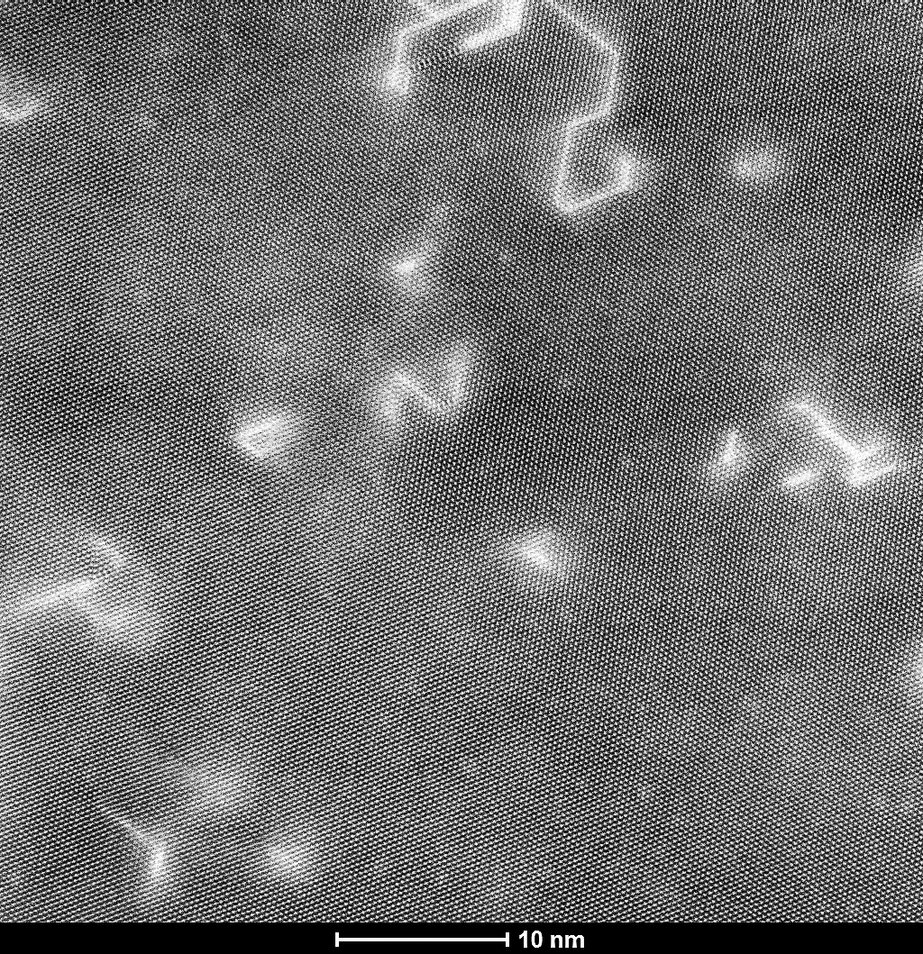
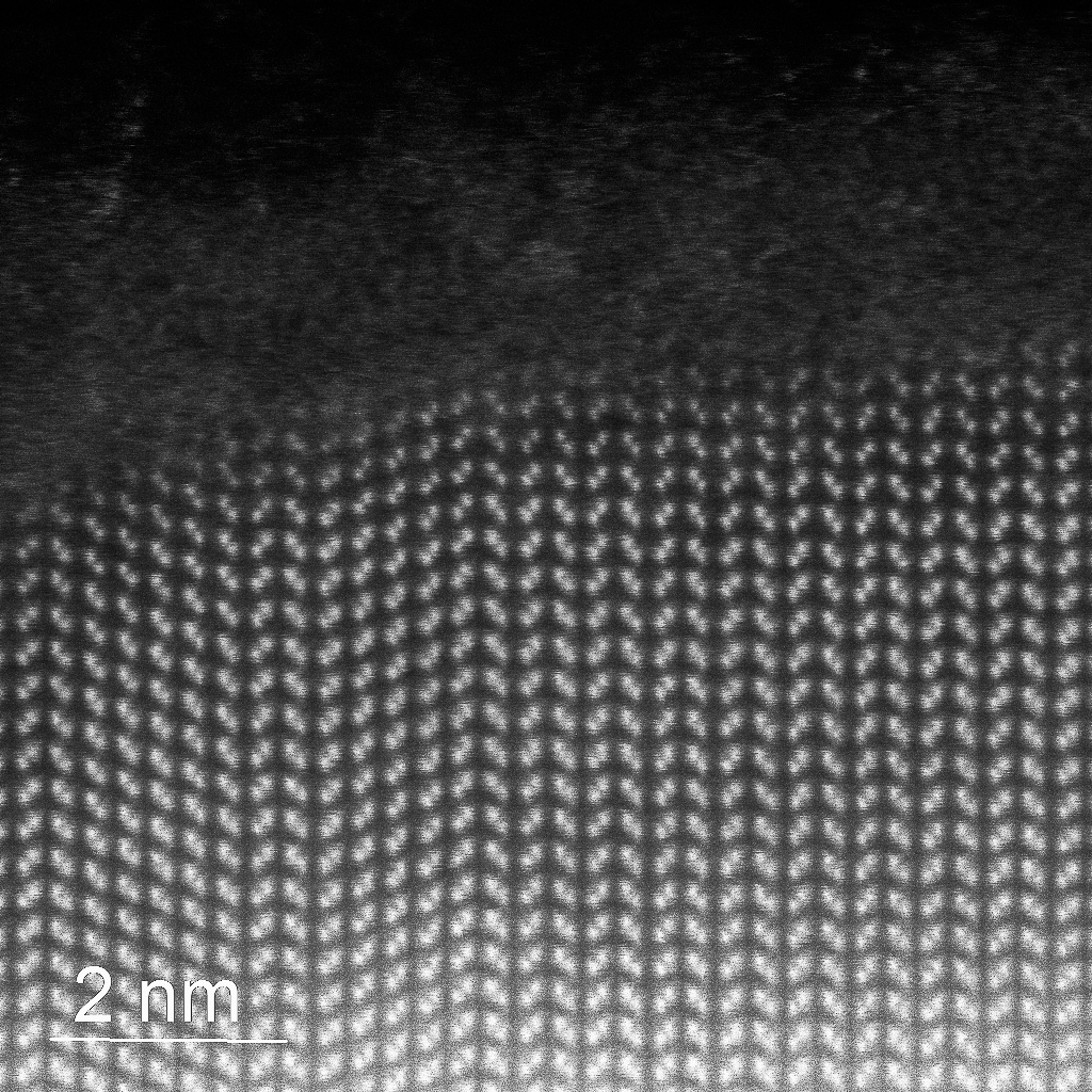
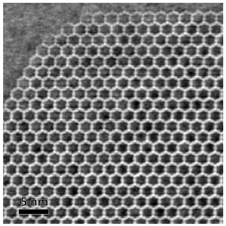
![Mo1.3TbAlC [010]](https://artemi.se/wp-content/uploads/2024/04/Mo1.3TbAlC-010.jpg)

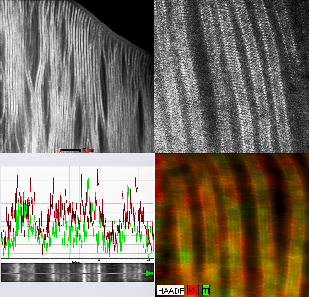
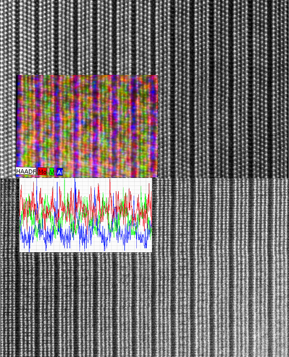
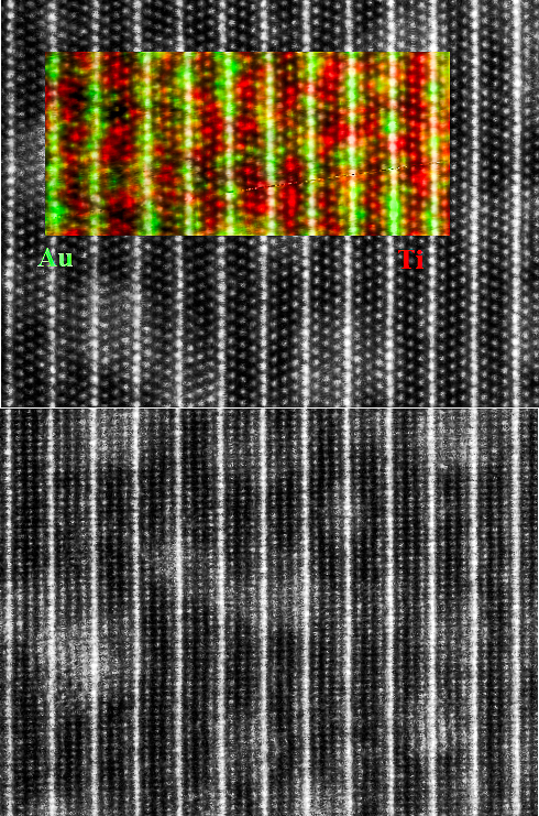
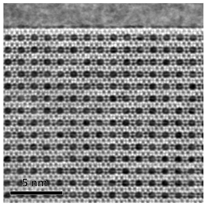
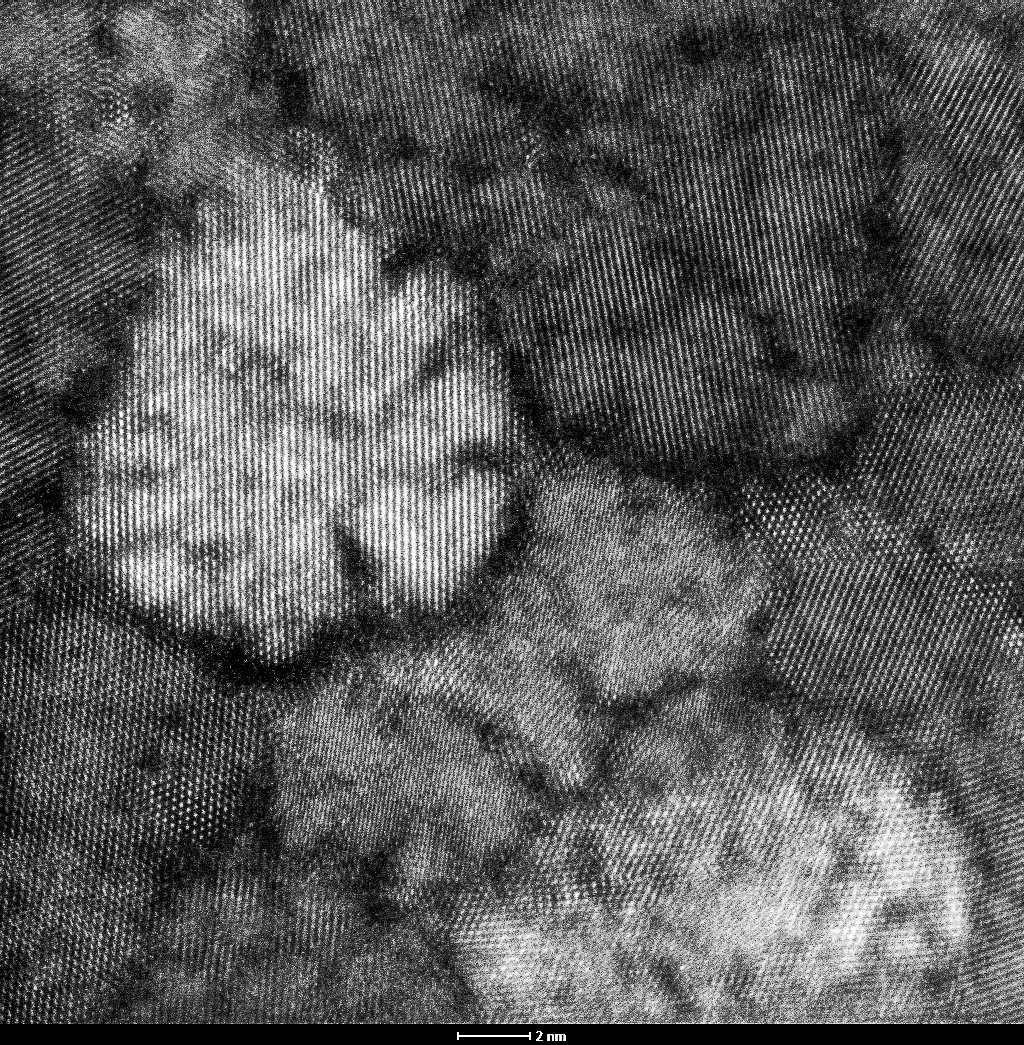
![Mo2TiAlC2 [11-20] mapping](https://artemi.se/wp-content/uploads/2024/04/Mo2TiAlC2-11-20-mapping.jpg)