News and Highlights
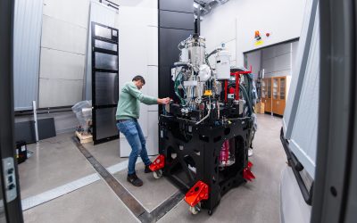
Arrival of Next-Generation Microscopy– New Iliad Ultra STEM Enables New Research Capabilities at ARTEMI and in Sweden
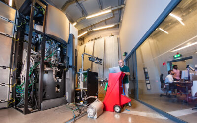
Arrival of Next-Generation Microscopy– New Iliad Ultra STEM Enables New Research Capabilities at ARTEMI and in Sweden The installation of the Thermo Scientific Iliad Ultra (S)TEM at Linköping University marks a significant advancement in ARTEMI’s analytical and...
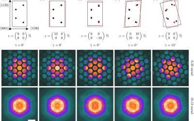
Neural Network-Enhanced PACBED for Characterizing Deformations in 2D van der Waals Materials
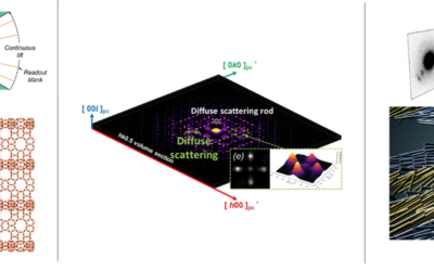
Atomic models of MoS2 and simulated PACBED patterns for five different strain tensor and rotation cases. For each case, the top panel illustrates the deformed unit cell (black) relative to the original unit cell (red) and specifies the strain tensor and rotation...
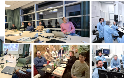
ARTEMI Staff Scientist Visit to Uppsala University
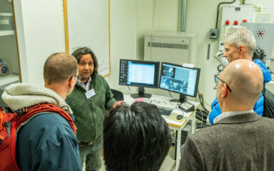
ARTEMI Staff Scientist Visit to Uppsala University The ARTEMI team meeting was hosted at the Ångström Laboratory, Uppsala University, on 19-20 November 2025. The first day focused on presentations highlighting ongoing transmission electron microscopy activities at...
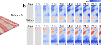
Ultrafast Imaging of a Propagating Photo-Driven Phase Transition Using 4D STEM
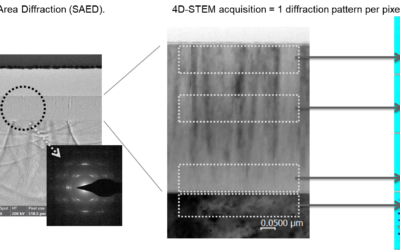
(a) A transient laser grating triggers a structural phase transition, resulting in different lattice structures in separate domains of the same lamella. (b) Ultrafast diffraction-contrast imaging using various virtual masks (right panel). Different virtual masks...
Three New PhD Theses Advance the Field of Electron Crystallography
Three New PhD Theses Advance the Field of Electron Crystallography Three recently defended PhD theses at Stockholm University have developed different aspects of electron crystallography, including advancements in terms of methods as well as structural analysis....
New Liquid Cell TEM Holder Enhances Electrochemical Research at Lund University
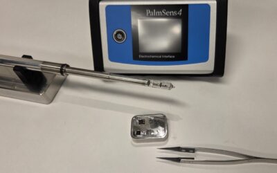
Figure 1. Newly delivered liquid cell transmission electron microscopy holder with potentionstat and MEMS chips.New Liquid Cell TEM Holder Enhances Electrochemical Research at Lund University Lund University has recently received a state-of-the-art liquid cell...
Microheater Controlled Crystal Phase Engineering of Nanowires Using In Situ Transmission Electron Microscopy
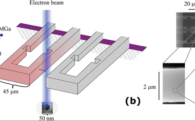
Schematic a) of two neighboring microheaters on a chip mounted in the ETEM. The illumination of a nanowire growing epitaxially from the microheater sidewall is indicated by the resulting image of the nanowire. The precursors are injected from two separate side ports...
ARTEMI Secures Continued Funding from the Swedish Research Council
ARTEMI Secures Continued Funding from the Swedish Research Council The Swedish Research Council has announced its decision on the research infrastructures to receive funding for the coming years. We are delighted to share that ARTEMI, the Swedish research...
The 9th International Workshop on Advanced and In Situ Microscopies of Functional Nanomaterials and Devices (IAMNano) 2025 was Held at Chalmers
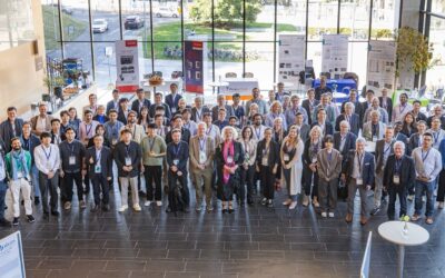
The 9th International Workshop on Advanced and In Situ Microscopies of Functional Nanomaterials and Devices (IAMNano) 2025 was Held at Chalmers The International Workshop on Advanced and In Situ Microscopies of Functional Nanomaterials and Devices (IAMNano) 2025 was...
Control of Phonons and Topology by Structured Light
Figure 1. (a) Schematic illustration of the experimental UEM geometry and sample excitation. (b) atomic structure mode of WTe2 in Td and T* phase. (c) DF imaging of an optically patterned structural phase transition.Control of Phonons and Topology by Structured Light...
In operando TEM analysis on the Solid State Battery materials (PEO+LiTFSI)
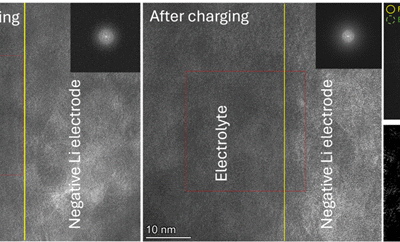
The formation of Li and Li₂O precipitates at the SEISEI layer growth in the solid state battery materials and Li mapping using STEM-EELSIn operando TEM analysis on the Solid State Battery materials (PEO+LiTFSI) A solid-state lithium battery for in-situ TEM observation...
Prof. Gunnar Svensson Steps Down After 40 Years in Science, SU’s EMC Welcomes New Director Prof. Tom Willhammar
Prof. Gunnar Svensson Steps Down After 40 Years in Science, SU’s EMC Welcomes New Director Prof. Tom Willhammar Professor Gunnar Svensson, Director of the Electron Microscopy Center (EMC) at the Department of Chemistry, Stockholm University since 2007, has decided to...
The first ARTEMI user meeting was held at Chalmers University of Technology
The first ARTEMI user meeting was held at Chalmers University of Technology The first ARTEMI user meeting was organized by Chalmers University of Technology (CTH) and held on February 5, 2025, both in-person in Gothenburg and online. This one-day event brought...
Oxidation of carbon nanomaterials using a nanoparticulate iron oxide catalyst: Direct observations in an electron microscope
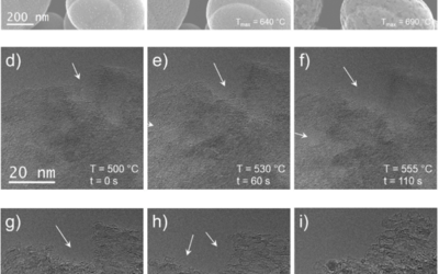
Oxidation of carbon nanomaterials using a nanoparticulate iron oxide catalyst: Direct observations in an electron microscopeOxidation of carbon black N990. Top row frames (a–c) were recorded in STEM mode using SE detector. Frame (a) was captured before oxidation...
Formation of Cr2C phase by Al extraction from a Cr2AlC using chemical etching-free methodology
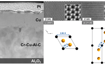
Formation of Cr2C phase by Al extraction from a Cr2AlC using chemical etching-free methodology MAX phases are a family of ternary nanolaminated compounds that have garnered significant attention due to their unique properties, which bridge the gap between metals and...
Mn-doped WSe2 as an efficient electrocatalyst for renewable energy production
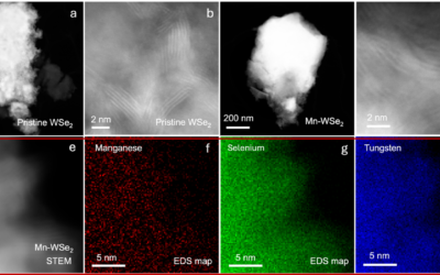
Mn-doped WSe2 as an efficient electrocatalyst for renewable energy production The ongoing energy crisis has made it imperative to develop low-cost, easily fabricated, yet efficient materials. Among transition metal dichalcogenides and other 2D materials, tungsten...
Ultrafast Imaging of Plasmon-Mediated Demagnetization Dynamics
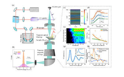
Ultrafast Imaging of Plasmon-Mediated Demagnetization Dynamics In a groundbreaking study, researchers at KTH employed Lorentz ultrafast electron microscopy (LUEM) to observe the spatiotemporal dynamics of ultrafast demagnetization mediated by surface plasmon...
Growth analysis of aluminum carbonitride (AlC3N) deposited by magnetron sputtering on monocrystalline sapphire substrate.
Growth analysis of aluminum carbonitride (AlC3N) deposited by magnetron sputtering on monocrystalline sapphire substrate Crystallinity control and its relation to the substrate is a central question in material design as it affects the physical properties of the...

