
Methods
Chalmers node
Chalmers specializes in utilizing ultra-high energy resolution electron energy loss spectroscopy (EELS) for various materials science and physics applications. The state-of-the-art JEOL mono NEO ARM200f at Chalmers provides exceptional energy resolution for EELS experiments that enables one to resolve features in EEL spectra that are inaccessible with standard EELS systems. This benefits experiments aimed at studying the optical, electronic, and phononic properties and elemental composition of a wide variety of material systems.
The Chalmers microscope utilizes a Gatan Imaging Filter continuum HR EELS spectrometer and a double Wien filter electron monochromator, which accepts the 0.6 – 0.7 eV energy spread of the electrons emitted from the Schottky field emission electron gun, and produces an electron beam with a tunable energy resolution down to <20 meV. Figure shows the EELS zero loss peak (ZLP) with different monochromator settings using a 40 keV beam energy. The ZLP shows the distribution of energy of the primary electron beam, and the full-width-half maximum (FWHM) of the ZLP is a standard metric for the energy resolution of an EELS system. The Chalmers system can tune the EELS energy resolution from ~0.7 eV down to ~20 meV, and is optimized for temporal stability so that this energy resolution can be maintained for many hours. Tuning the energy resolution also modifies the electron beam current, as shown in the inset figure. Even with full monochromation and a <20 meV energy resolution, it is still possible to get a beam current of a few tens of pA, which is enough for many experiments.
The monochromated EELS capabilities can be utilized in parallel with the advanced aberration correction systems (double corrected: HRTEM and STEM) to enable combined atomic spatial resolution and ultra-high energy resolution. This opens many exciting experiments aimed at resolving physical phenomena and properties of materials at the atomic scale.

Energy resolution of the primary electron beam with different monochromator settings
KTH node
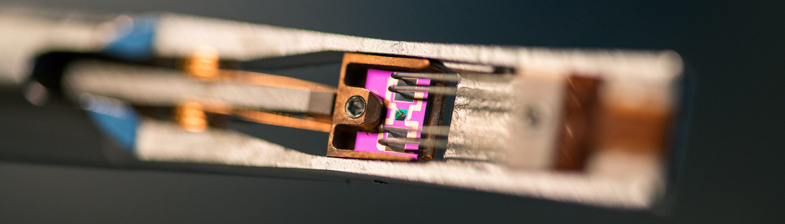
In a UEM of KTH node, we can operate in two modes: in-situ mode and time-resolved mode. In in-situ mode, a fs-laser pulse is directed towards the sample to initiate the desired change in state (chemical reaction, phase transition, melting, etc.), then a continuous electron beam thermally-emitted from LaB6 cathode illuminates the sample under or after laser excitation.
Then, the information of the sample state is in-situ recorded by the CCD camera. In time-resolved mode, a femtosecond laser pulse (in UV wavelength) is steered into a modified column of a TEM and directed onto the cathode to generate a few electrons ultra-short electron pulse through a photoemission process. The femtosecond electron pulse travels through the column to the sample. A second laser pulse (from the same source) is directed through an adjustable optical path towards the sample to trigger ultrafast dynamics (phase transition, mechanical motion, spin dynamics etc.), thus enabling a temporal reference point (time zero) for the changes that occur.
By fine-tuning, at the femtosecond time scale, the relative arrival time of the laser pulse (pump) and electron pulse (probe pulse), a series of micrographs (or diffraction patterns) can be recorded during the process of change in state and information on many aspects of its dynamic or transient properties can be obtained.
The UEM in this design can produce nanometer resolution in the imaging mode, a precision of a few thousandths of an Ångström in diffraction mode, and that with a time resolution of sub picosecond. This is 10 orders of magnitude better than conventional microscopes, which are limited by the video-camera rate of recording.
")
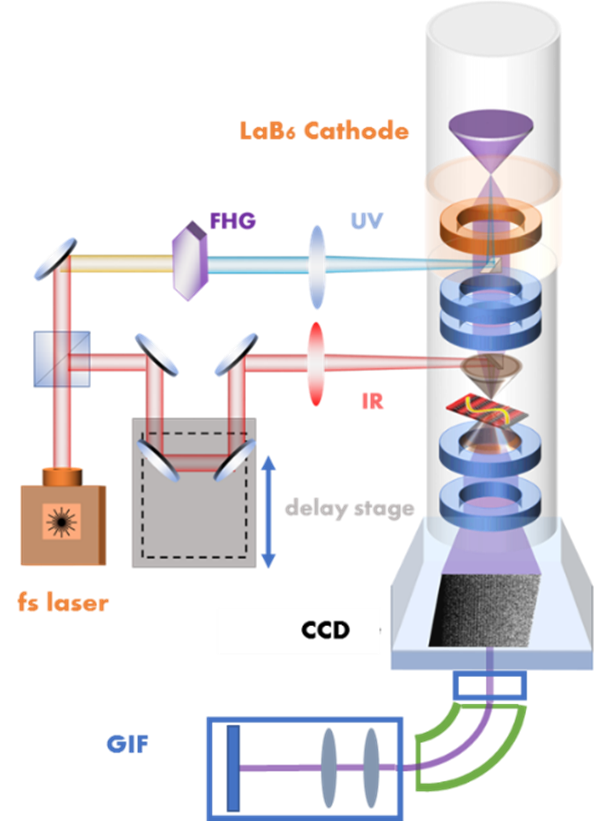
The schematic illustration of the UEM in KTH
Lund University node
The Lund node for ARTEMI has two specialist methods that we highlight here.
The first method is Environmental TEM or ETEM. TEM is normally a high-vacuum technique, but through differential pumping it is possible to create an “environment” by confining reactive gases to the sample area. With the sample mounted on miniaturized heating chips, we can observe the resulting reactions between gases and solids/liquids including growth of nanowires or microstructural changes. The observations take all the usual forms, i.e. imaging — TEM or STEM — diffraction and energy dispersed X-ray spectroscopy. They are performed in real-time with a time resolution of around 10 ms. The microscope is equipped with an aberration corrector for TEM images which provides a point-to-point resolution better than 1 Å over a large field of view. The main activity has been imaging the atom-by-atom growth of semiconductor nanostructures. In this role, the ETEM at nCHREM is world-unique by incorporating an industry standard CVD (Chemical Vapor Deposition) system for delivering the gases. We are, however, also studying combustion processes in nano-carbons, high-temperature degradation and oxidation processes in ceramic surface coatings, and brazing processes for high-performance steels. These last two examples demonstrate that ETEM is also relevant for “bulk” materials, after thinning and polishing the bulk sample to electron transparency.
The second specialist method in Lund is CryoEM for soft materials. By rapid freezing of a thin layer of the aqueous sample, dispersions of biomolecules or soft materials can be preserved in their natural hydrated state, albeit immobilized in amorphous ice. The frozen sample survives in the vacuum of the TEM, and is viewed with low dose techniques to minimise electron beam damage. Other CryoEM microscopes are designed for single particle analysis (SPA) and the 3D structure determination of biomolecules. The Lund CryoEM is mainly used in research areas where the “particles” are not identical: e.g., molecular aggregates, lipid vesicles, foods, clays, and soft materials in general. The particles are then analysed individually. 3D information can still be retrieved through cryo-tomography, whereby images are recorded while rotating the sample, and subsequently combined. Elemental maps may also be obtained via energy filtered imaging.
Lund also offers regular methods which include STEM-EDX on the 300kV TEMs, HRTEM with aberration correction, and also SEM-EDX as a support to the TEM studies on a sample.

Schematic diagram of the gas handling system in the Lund ETEM. Gases are supplied to the ETEM via the specimen holder or via injectors at the sample area of the column. An ex situ chamber allows initial tests, or exposure to higher pressures

Two images that show in situ growth of a GaAs nanowire. The long white line in the GaAs nanowire acts as the reference point for the two images: to the right is twinned zinc blende (cubic) GaAs while to the left is the growing wurtzite (hexagonal) GaAs. Two atomic layers, total spacing 6.5 Å, have grown in the 14 second time interval, and the arrow indicates a third layer starting to grow. Gases (not visible) supply the Ga and As atoms via the dome-shaped gold catalyst particle
Stockholm University Node
SU is internationally leading in electron crystallography, and has developed a number of techniques for 3D electron diffraction (3DED). 3DED data collection by rotation electron diffraction (RED) or continuous RED (cRED) has been established and used on a routine basis for phase and structural analysis. Compared to X-rays, electrons interact with matter a few magnitudes stronger, and ED can study the sub-micron or nano-sized crystals. In addition, ED requires a lower electron dosage on the sample than conventional high-resolution TEM imaging does and therefore causes less specimen damage.
RED method combines goniometer tilt and electron beam tilt to collect 3D diffraction data set. A series of ED patterns of a single crystal was recorded at different tilt angles by tilting the holder done by the goniometer and in a parallel electron beam condition. In this stepwise acquisition, the tilt angle step can be 0.5º – 2º. This goniometer tilt step is followed by electron beam tilt, in order to fill the gap between the tilt. The electron beam tilt is done by the microscope deflector, and the step can be <0.1º. Another approach is to collect ED patterns while the crystal is being tilted by the goniometer continuously. This is known as continuous RED (cRED), as well as MicroED. Such strategy can ensure the sample having minimum total dose that is most commonly used for study electron beam sensitive materials, e.g. organic molecules, proteins, etc. The reconstructed 3D data set can already provide the information of unit cell, and the processed results can be input into different existing packages for structure refinement, e.g. SHELXS-97 or SIR2011.
Furthermore, a high-throughput technique – SerialED allows automated particles searching (>3000 particles/hour) and automated cRED data collections. In this fully automated method , automatically crystal screening and collecting 3D ED data from hundreds of crystals in a product are able to perform phase analysis and structure determination of products with multiple phases and various sized crystals without human intervention.

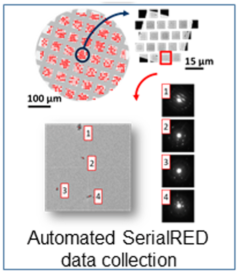
The schematic illustration of the Rotation Electron Diffraction (RED) and SerialRED
Uppsala University node
In a TEM laboratory of the Uppsala University node, one of our foci are the spectroscopy techniques of EDS and EELS. They are available on our probe correction Titan-Themis TEM. The state-of-the-art energy filter was installed in 2023 and is equipped with a 4K CMOS camera and a hybrid-pixel camera. The latter camera operates close to an electron efficiency of 1 and therefore close to shot-noise limit. This is very important for the acquisition the small intensities that we obtained in our EELS measurements at atomic resolution. Furthermore, the same camera can acquire up to 13.000 full frame images per second which makes it possible to acquire 4D-STEM data such as needed to obtain diffractions scans or dynamic phase contrast (DPC) mapping. The latter technique is used to visualise among else magnetic and electrical fields. To analyse energy materials, we have available low and high temperature sample holders as well as in-situ biasing and electrochemical sample holders.

