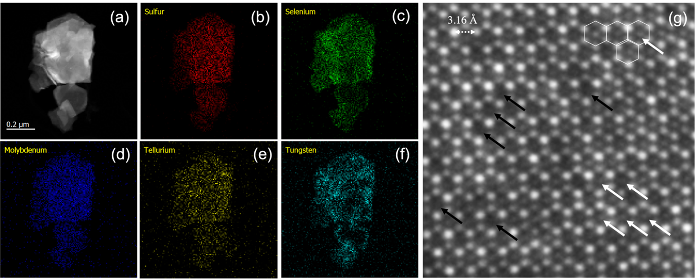
Composition and structure of a 2D TMD alloy flake consists of Mo, W, S, Se and Te. (a) Overview STEM ADF image of the flake. (b)-(f) STEM-EDS elemental maps of S, Se, Mo, Te, and W, respectively. (g) High resolution STEM ADF image showing the atomic structure of the 2D alloy. White hexagons are used to mark the basic structure units. White arrows indicate the existence of atoms at the center of the hexagons, while black arrows show areas where there are no atoms at the center of the hexagon units.
Case study: Structure characterization of 2D TMD alloys at the nanometer and atomic scales
Transition metal dichalcogenides (TMDs) have attracted great interest in the last decade not only because they possess outstanding electrical, mechanical, and optical properties, but also due to their layered structure that can be used to fabricate atomically thin two-dimensional (2D) materials. TMDs normally have a chemical formula MX2, where M is a transition metal element including Mo or W, and X is a chalcogen element such as S, Se, or Te. Though possessing similar lattice structures, pure phase 2D TMDs, such as MoS2, WS2, and MoTe2, have unique properties, such as band gap and exciton binding energy. One promising method to engineer the 2D TMD structure and achieve desired functions is forming alloys between the pure phase TMDs. The structure of the TMD alloys (especially when more than three elements are involved) is still not well understood due to the small differences in forming energies between the different phases of the TMDs. In particular, the atomic structure and chemical homogeneity of the 2D alloys are of high interest for understanding the alloying process in 2D TMDs.
Scanning transmission electron microscopy (STEM) and energy dispersive X-ray spectroscopy (EDS) were applied to unveil the nanometer and atomic scale structure of 2D (Mo/W)(S/Se/Te)2. By scanning high energy electron beam over a sample area and acquire an EDS spectrum at each beam position, STEM-EDS measurements provide a powerful way to directly map the elemental distribution in the 2D materials at the nanometer and sub-nanometer scale. High resolution STEM annular dark field (ADF) imaging allows direct visualization of the atomic arrangement in the alloy system. The measurements were performed using a JEOL monochromated ARM200F TEM, which is equipped with a double-Wien monochromator, a probe Cs corrector, a double silicon drift detector (SSD) for EDS, an image Cs corrector, as well as multiple STEM ADF and bright field (BF) imaging detectors.
STEM-EDS mapping shows the distribution of Mo, W, S, Se, and Te in a nanoscale flake of the 2D alloy (a)-(f). All the elements are distributed over the whole flake, despite nanoscale inhomogeneities. Quantification of the EDS data verifies that the composition of the 2D alloy is consistent with the nominal composition.
High resolution STEM ADF image unveils the atomic scale structure in the alloy flake (g). The STEM ADF image contrast is related to atomic number roughly by Z𝛼 (1<𝛼<2). STEM ADF image directly reveals that there is composition and structure inhomogeneity at the atomic scale. By considering the basic structure units as hexagons, such as those marked in (g), atomic structure inhomogeneity is manifested as the presence of atoms at the center of the hexagon units in some areas and the absence of them in other areas. The variation in the image intensity of the atomic columns at the corners of the hexagon units indicates the uneven distribution of the elements in the flake.
