
Beyond Elemental Mapping: The Power of STEM-EELS
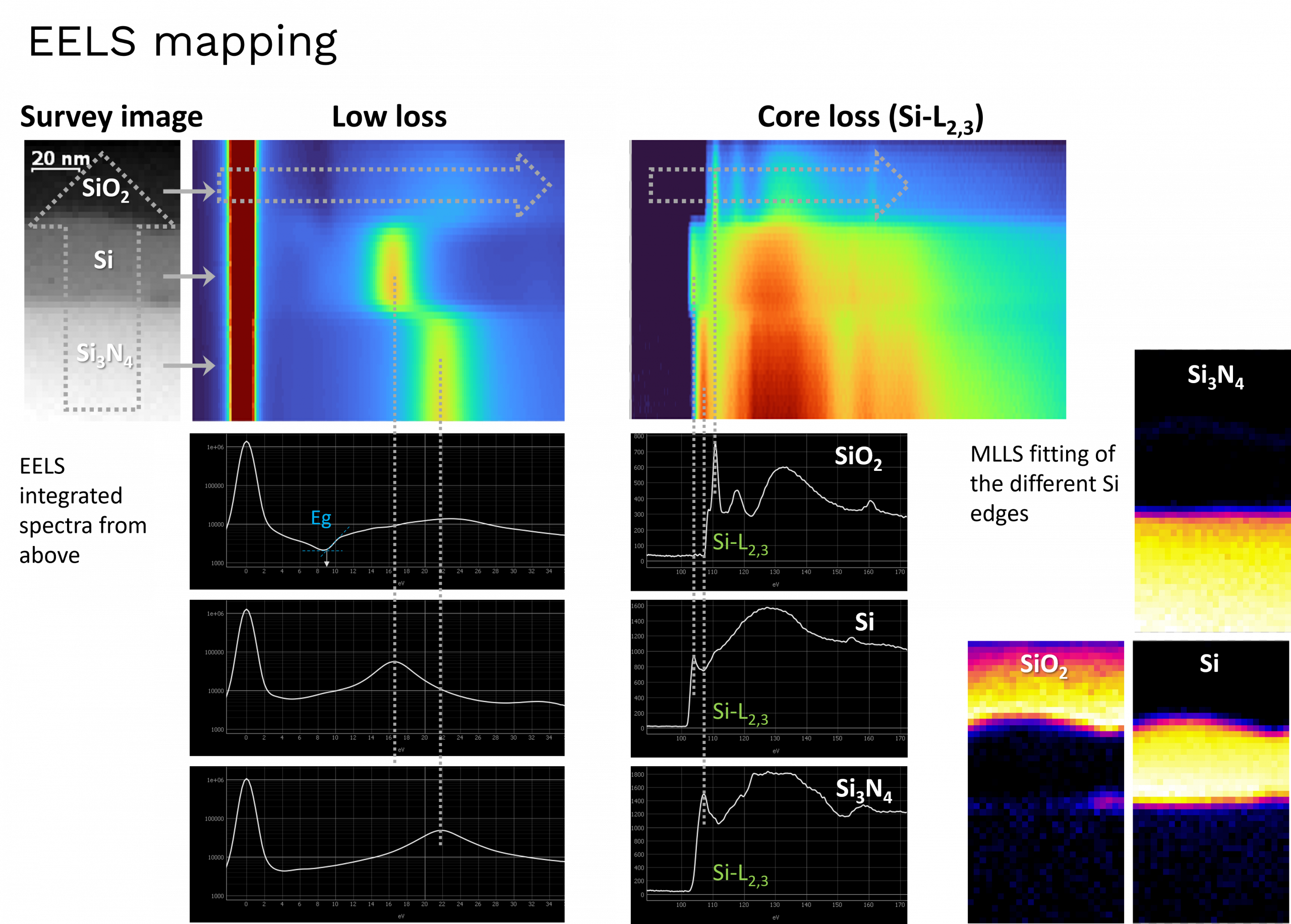
Scanning transmission electron microscopy combined with electron energy-loss spectroscopy (STEM-EELS) enables comprehensive nanoscale characterization within a single acquisition. While energy-dispersive X-ray spectroscopy (EDS) may primarily reveal variations in silicon concentration, EELS goes a step further, uncovering the underlying chemical phases, bonding environments, and fine electronic structures.
Both chemical shifts of the Si-L₂,₃ edge and characteristic energy-loss near-edge fine structures (ELNES) can be used to identify different phases within a sample. Furthermore, multiple linear least-squares (MLLS) fitting allows the spatial distribution of these phases to be mapped by identifying regions with similar spectral signatures. With sufficient energy resolution, EELS can also provide insights into the local band gap.
These measurements were performed at the Uppsala ARTEMI node, where recent advances in direct electron detection, including the ELA detector from DECTRIS, combined with the CEOS energy filter and Panta Rhei software, enable the acquisition of exceptionally high-quality EELS datasets with remarkably low noise levels.
These capabilities highlight the advanced analytical possibilities available at the Uppsala ARTEMI node, allowing researchers to explore chemical and electronic structures at the nanoscale in greater detail than conventional elemental mapping alone.